Have you ever wondered how your computer works?
A crucial element in making it all happen is the Printed Circuit Board (PCB).
This humble component acts as the backbone of your computer.
It connects all the different parts to ensure they work well together.
Without the PCB, your computer wouldn’t function properly.
So, next time you switch on your device, thank the small but mighty PCB for keeping everything running smoothly.
Table of Contents
Definition of PCB
A printed circuit board is a vital part of electronic devices. It serves as a base for assembly of electronic circuits.
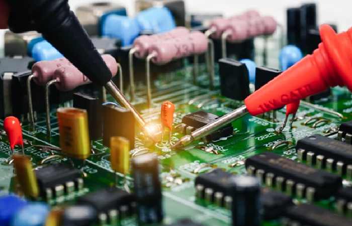
PCB assembly involves arranging copper tracks on insulating layers (substrates). These tracks connect components like resistors, capacitors, and integrated circuits.
Designing a PCB includes creating pathways for circuits. This uses methods like surface mount technology or point-to-point wiring.
Materials such as solder masks and legends insulate and label the PCB.
PCBs have precise wiring density to handle the complex circuitry in modern devices.
Multilayer PCB development allows for more components by stacking layers and using microvias for signal routing.
Importance of PCB in Computers
The printed circuit board is vital in creating electronic devices like computers.
It connects different components in a computer system, such as integrated circuits, resistors, and capacitors.
The PCB’s design and composition are essential for computers’ efficiency and reliability.
PCBs have layers of copper tracks, pads, and vias on an insulating substrate, forming complex electrical circuits.
Conductive tracks on the PCB allow wiring and connection of various components, while solder mask and legend provide insulation and labeling.
PCB technology also allows for multilayer boards that increase wiring density and save space.
In short, PCBs are essential for electronic devices, providing circuits for computers to work efficiently.

Construction of PCB
Materials Used in PCB
Materials commonly used in PCB construction are:
The thickness of copper in a PCB affects its function. It impacts electrical conductivity and heat dissipation.
Drilling and vias are essential in PCB design. They create pathways for components to connect and allow for layer integration in a small space.
These components and methods are crucial in developing electronic devices. They enable the creation of complex circuits for various electronic applications.
Layers of a PCB
Multiple layers in a PCB design are important for making electronic devices efficient. The number of layers impacts performance by providing space for circuits, tracks, and components. Layers are connected using methods like Vias, which help devices work correctly. A typical layer includes substrate, copper, and traces for electrical signals. PCB assembly design includes insulation layers to prevent shorts and allow for dense wiring.
Multilayer technology lets devices integrate components, including resistors and capacitors. It improves functionality and power distribution. Stacking layers, solder masks, and legends are crucial for making electronic products. This makes PCB design a key part of modern electronics.
Component Mounting on PCB
Mounting components on a Printed Circuit Board is important for computers to work. It involves attaching electronic parts to the PCB. These parts include resistors, capacitors, and integrated circuits. This creates the electrical pathways needed for the device to function.
The PCB is a base made of insulating materials with copper layers that form the necessary circuits. The thickness of the copper is vital as it affects the board’s ability to carry current without issues.
Drilling holes and creating vias in the PCB are crucial steps. This allows components to connect on different layers. It supports the wiring and signal transmission that electronics need to work.
The methods for mounting components are important. These include surface mount technology and through-hole assembly. They are key to making reliable electronic products.
Functionality of PCB in Computers
Connection Between Components
Connecting components on a printed circuit board is important for electronic circuits to work in a computer.
The layout and design of a PCB affect how well these connections work. Factors like copper thickness, drilling, and vias are important.
The copper tracks, pads, and vias on the PCB create paths for moving electrical signals, helping power and data flow in the device.
Insulating layers, solder resistors, and legends on the PCB prevent short circuits and ensure the circuit works.
A good PCB assembly is crucial. It makes devices work, and computers function well.
Vital Function of PCB
A Printed Circuit Board helps computers work by connecting electronic components. The design includes layers with copper tracks for electrical circuits. Components like resistors, capacitors, and circuits are soldered using vias and pads. The PCB’s substrate insulates the wiring and maintains circuit density.
Advanced assembly methods, like surface mount assembly, allow us to make complex electronic devices. They have PCBs. PCBs are crucial in computers. They ensure the smooth flow of electrical signals between components. This flow lets the system work.
What is the Function of PCB in a Computer?
Copper Thickness Importance
Copper thickness is important in PCB assembly. It affects conductive properties and overall circuit performance.
The amount of copper in a PCB affects conductivity and signal transmission. This includes resistors, capacitors, and integrated circuits.
Copper layer thickness impacts wiring density, which affects device functionality and reliability.
When designing a PCB, consider power needs and signal quality. Also, consider manufacturing methods to choose the right copper thickness.
Copper pads, traces, vias, and tracks are vital. They connect components and ensure the device works.
Drilling and Vias in PCB
Drilling and vias in PCB assembly are essential for designing printed circuit boards. These components help create electrical connections between different layers of the PCB.
Tracks connect components and circuits by drilling holes in the substrate. The holes let conductive copper pass through. Vias act as channels for signals. They travel through the board, improving electronic devices.
This method enhances component density and allows for more complex circuits to be integrated. It aids in developing multilayer PCBs that contain many electronic components.
In electronics manufacturing, drilling, and vias are crucial. They make intricate wiring and circuit design in innovative products.
Composition and Design of PCB
Use of Laminates in PCB Design
Laminates in PCB design have many benefits. They provide a stable base for mounting electronic components, such as resistors, capacitors, and integrated circuits. Using laminates allows for making multilayer PCBs. They have many copper tracks, enabling dense wiring for complex circuits.
Composition of Copper in PCB
Copper is important in a PCB because it conducts electricity well.
It helps transfer electrical signals between parts of the board.
Copper layers in a PCB create traces, tracks, and pads for carrying the current.
The design places copper elements for proper connectivity.
Vias with copper connections link different layers in a multilayer PCB.
Copper provides a surface for soldering components like resistors and capacitors.
It also acts as a conductive path for transmitting signals between devices.
Modern technology optimizes copper composition for better conductivity and functionality in PCBs.
Summary
Printed circuit boards (PCBs) are important for computers. They help connect electronic components and allow them to communicate. PCBs ensure that signals and power flow well on the computer. Computers need PCBs to work correctly.

